BHUBANESWAR, India – The eastern Indian state of Odisha has allocated 1,000 acres of land near its capital for the development of a dedicated Odisha semiconductor cluster, a significant move aimed at attracting global chipmakers. This initiative positions the state as a serious contender in India’s national strategy to build a self-reliant electronics manufacturing ecosystem and reduce its dependence on foreign imports.

The land is located in Gothapatna, a key industrial and educational area on the outskirts of Bhubaneswar. Officials state the site’s strategic proximity to academic institutions and existing infrastructure is designed to create a comprehensive environment for research, development, and large-scale production of semiconductors. The move is part of a broader effort to transform Odisha into a leading hub for the electronics industry in South Asia.
A Strategic Bid for India’s Tech Future
The creation of the Odisha semiconductor cluster is a direct response to the central government’s ambitious India Semiconductor Mission (ISM). Launched with a $10 billion incentive package, ISM aims to establish India as a global player in a sector dominated by Taiwan, South Korea, and the United States. The Indian government is offering substantial financial support, including up to 50% of project costs, to companies willing to establish manufacturing facilities in the country.
“By providing plug-and-play infrastructure, we are signaling to the world that Odisha is ready for business,” said Tusharkanti Behera, Odisha’s Minister for Electronics & Information Technology, in a statement released by his office. “Our goal is to attract a major anchor investor that can catalyze the development of a full ecosystem, from design and fabrication to assembly and testing.”
Experts see this as a calculated move by Odisha to compete with other Indian states like Gujarat and Tamil Nadu, which have also been aggressively courting foreign investment in the chip sector. Last year, American memory chip giant Micron Technology announced plans to build a $2.75 billion assembly and test facility in Gujarat, marking a major win for the national mission.

“The competition among states is fierce,” stated Dr. Anish Kapoor, a technology policy analyst at the New Delhi-based Observer Research Foundation. “Success will depend not just on offering land and financial incentives, but on ensuring a seamless supply of critical resources like ultra-pure water and uninterrupted power, which are non-negotiable for semiconductor fabrication.”
Building an Ecosystem from the Ground Up
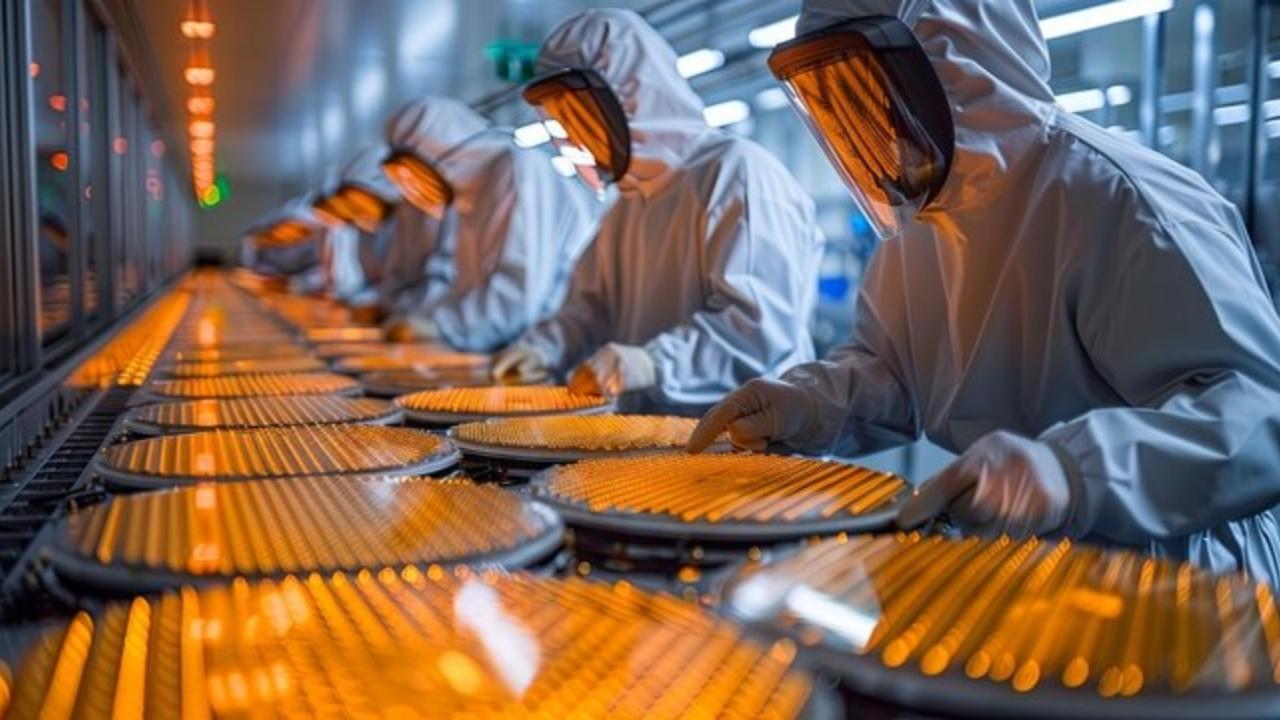
Semiconductor manufacturing is one of the most complex and capital-intensive industries in the world. A “fab,” or fabrication plant, can cost billions of dollars to build and requires a highly specialized workforce and a stable supply chain of gases, chemicals, and equipment. Odisha’s plan acknowledges these challenges by co-locating the cluster near top educational institutions.
Infrastructure and Talent Development
The chosen site in Gothapatna is close to the International Institute of Information Technology (IIIT) Bhubaneswar and other engineering colleges, which the government hopes will provide a steady stream of skilled talent. The state’s industrial policy also includes provisions for customized training programs to prepare a local workforce for the specific demands of India chip manufacturing.
“We are not just offering land; we are offering a partnership,” a senior official in the state’s industrial development corporation told reporters. “This includes working with investors on workforce development, infrastructure needs, and regulatory clearances to ensure a swift project launch.”

Overcoming Global Challenges
The global push for semiconductor supply chain diversification, accelerated by the COVID-19 pandemic and geopolitical tensions, creates a window of opportunity for new players like India. Governments in the U.S. (with its CHIPS Act) and the European Union are also offering massive subsidies, intensifying the global competition for investment.
For Odisha, attracting a large-scale chip fabricator remains the ultimate goal. However, industry analysts suggest the state could also find success by targeting companies in related sectors, such as Assembly, Testing, Marking, and Packaging (ATMP), or by focusing on compound semiconductors used in the automotive and power electronics industries.
The government has confirmed it is already in preliminary discussions with several international firms, though no names have been officially disclosed. The next few months will be critical as state officials engage in international roadshows to market the Odisha semiconductor cluster to potential investors. The success of this initiative could redefine the state’s economic landscape and play a crucial role in India’s quest for technological self-reliance.
Odisha Emerges as Major Semiconductor Hub With ₹2,066 Crore Investment
Odisha Literary Fest 2025 Begins: The Opening Session Everyone Is Talking About!
Land Rush for Tech: Odisha Designates 5,500 Acres for IT and ESDM Development
FAQs
1. What is a semiconductor cluster?
A semiconductor cluster is a geographically concentrated area that hosts a network of companies and institutions involved in the semiconductor industry. This includes design firms, fabrication plants (fabs), assembly and testing facilities, equipment suppliers, and research institutions that work together to create a synergistic ecosystem.
2. Why is India focusing on chip manufacturing?
India is focusing on India chip manufacturing to enhance its economic and national security. By building a domestic industry, the country aims to reduce its heavy reliance on imports for critical electronic components, insulate itself from global supply chain disruptions, and capture a share of the rapidly growing global semiconductor market.
3. Who are the major players in the global semiconductor industry?
The global semiconductor industry is currently dominated by companies from Taiwan (like TSMC), South Korea (like Samsung), and the United States (like Intel and NVIDIA). These countries lead in different segments, from advanced chip manufacturing to design and equipment.